Nanoscience and Engineering center, Maulana Azad National Institute of Technology (MANIT), Bhopal-462051 (M.P), INDIA
Corresponding author Email: gagankanttripathi@gmail.com
Article Publishing History
Received: 18/06/2019
Accepted After Revision: 12/09/2019
Electronic state of a material is an arrangement allowed by the laws of quantum mechanics of electrons within an atom, molecule or system of molecules. Low-cost nano materials single wall carbon nano tubes and multi walled carbon nano tubes based on semiconductor devises. In case of a metal, the quasi-continuous density of states in the valence and the conduction bands splits into discrete electronic levels, the spacing between these levels and the band gap increases with decreasing particle size. Discussion of electronic and optical properties of carbon nano tubes depends upon size, morphology and synthesis methods. They are smaller than the wavelength of visible light and a hundred-thousandth times the width of a human hair. At this range, unusual properties of materials emerge out that can be applied to yield technologies and products with undividedly new abilities and applications.
Engineering, Quantum dots, Morphology, CNT.
Tripathi G. K. Engineered Nanomaterials and Their Properties : A Review. Biosc.Biotech.Res.Comm. 2018;11(3).
Tripathi G. K. Engineered Nanomaterials and Their Properties : A Review. Biosc.Biotech.Res.Comm. 2018;11(3). Available from: https://bit.ly/2ltwbMS
Introduction
Engineered Electronic State of Nanomaterials
Nanomaterials are the soul of nano engineering and nanotechnology. These materials possess at least one dimension in the 10–9 m, nanometer, range which is one billionth of a meter. In nanomaterials surface-to-volume ratio increases (Siegel et al, 1993; Collins et al, 2000, Alagarasi 2011).The number of atoms on the surface may be similar to or higher than those located in the crystalline lattice core and the surface properties are no longer negligible. When no other molecules are adsorbed onto the nano crystallites, the surface atoms are highly unsaturated and their electronic contribution to the behavior of the constituent particles is absolutely diverse from that of the inner laying atoms. Electronic State of a material is an arrangement allowed by the laws of quantum mechanics of electrons within an atom, molecule (or system of molecules) (Bate et al, 1975; Frolov et al, 2001).
Fig. 1.1 and 1.2 give the electronic structure of bulk semiconductors and low dimensions respectively. In bulk, the electrons in conduction band and holes in valence bands have degree of freedom in all 3 dimensions.
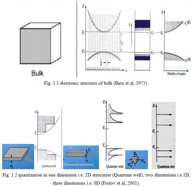 |
Figure 1.2: Quantization in one dimension i.e. 2D strucutres (Quantum well), two dimensions i.e.1D, three dimensions i.e. 0D (Frolov et al, 2001). |
As the size of the nanoparticle increases, the band structure evolves gradually i. e., molecular orbital change to delocalized band states. Figure 1.3, shows the size quantization effect which leads to conversion between a bulk metal or semiconductor, and cluster species. In case of a metal, the quasi-continuous density of states in the valence and the conduction bands splits into discrete electronic levels, the spacing between these levels and the band gap increases with decreasing particle size (Mekala et al, 2000; Bogue at el, 2010; Medintz et al, 2005). In the case of semiconductors, a band gap already exists in the bulk state. This band gap increases as the size of nanoparticle decreases and the energy bands gradually convert into discrete molecular electronic levels (Kim et al, 2011; Patil et al, 2012; Sharma et al, 2013 Tripathi et al, 2016).
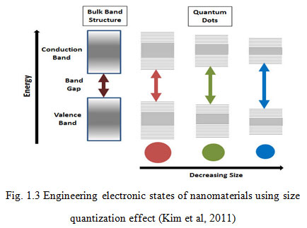 |
Figure 2: Engineering electronic states of nanomaterials using size quantization effect (Kim et al, 2011) |
Engineered Nanomaterials are the manipulated matter on the nanoscale. Electronic states of nanomaterials can be engineered by tuning the following parameters: Size, aggregation or dispersion state and the extent of dissolution.
Size, morphology, and aggregation state
Some Engineered nanoparticles dispersions may have narrower size distributions than their naturally occurring counterparts as nanomaterials produced anthropogenically are tailored for specific, size-dependent properties; whereas, naturally occurring nanomaterials generally will not have such restrictions. One other technique capable of sizing nanoparticles is single particle inductively coupled plasma mass spectrometry (SP-ICP-MS), which can provide element-specific information about individual particles that are ablated in the plasma (Pace et al, 2012; Mitrano et al, 2012 Tripathi et al, 2016).
SP-ICP-MS has been employed to size a diversity of NMs such as silver, gold, and metal oxide particles in various complex media (e.g., wastewater, bovine serum albumin). Although this technique requires information regarding particle shape and is currently hemmed in by the nano particle’s size (Pace et al, 2011; Reed et al, 2012).
Dissolved ions vs. nano particulate
In spite of incidental and naturally occurring nanomaterials, various samples in environment comprise a high concentration of dissolved ions that, when using chemical analysis-based methods, may overestimate the amount of material present in nanoparticle form. One way of distinguishing between nanoparticles and dissolved forms of the material is through filtration methods, whereby particles can be size-fractionated, with the remaining fraction composed of dissolved ions. Similarly, centrifugation can put to use where particles may settle out under the centrifugal force, and the supernatant that is decanted, should contain the dissolved forms of the material. As the dimensions of the material is reduced the electronic properties change radically as the density of states and the spatial length scale of the electronic motion are reduced with decreasing size (Liu et al, 2008; Chen et al, 2012; Tripathi et al, 2016).
Table 1: Some synthesis methods and characteristics of engineered nanoparticles
| Process | Elemental Composition Examples | Characteristics |
| Chemical reduction | Zerovalent metals Au, Ag, Fe | Mono-elemental in composition, (Au, Ag) monodisperse and often as spheres or wires |
| Sol-gel | Metal oxides SiO2, TiO2, ZnO, CeO2 | Single metal, moderate polydispersity, 2D and 3-D nanoscale dimension |
| Solvo synthesis | Semiconductors CdSe/ZnS, CdTe | Multi-metal composition, low polydispersity |
| Vapor-phase | Carbonaceous materials, metal oxides Carbon nanotubes, fullerenes | Polydisperse, 2-D nanoscale dimension |
| Organic synthesis | Multi-functional polymers | Carbon-based, monodisperse, 3-D nanoscale dimensions |
Electrical properties
Electrical Properties of nanomaterials hold forth the essentials of electrical conductivity in nanorods, nanotubes, nanocomposites and CNT and optical properties of nanorods as well. The low dimensions of a nanowire and measurement of the electrical current at a constant applied voltage is one of the methods to validate the quantum conductance. Here with decreasing diameter of the wire, the number of electron wave modes contributing to the electrical conductivity becomes increasingly smaller by well-defined quantized steps (Liang et al, 2011; Benn et al, 2010; Danniel et al, 2004). In CNT’s, single electron wave mode is observed that conducts the electrical current. Different lengths and orientations of the carbon nanotubes provide two information: (i) the influence of carbon nanotube length on the resistance; and (ii) the resistances of the different nanotubes.
Selected Application of Engineered Nanomaterials
Nanomaterials have extensive application in the field of electronics, fuel cells, batteries, agriculture, food industry, and medicines, etc. Nanomaterials holds supercilious chemical, physical, and mechanical properties and of their exceptional formability.
Fuel cells
A fuel cell is an electrochemical energy conversion device that converts the chemical energy from fuel (on the anode side) and oxidant (on the cathode side) unswervingly into electricity. The soul of fuel cell is the electrodes. The structure of electrode must provide plenty surface area, maximum contact of catalyst, reactant gas and electrolyte, facilitate gas transport and provide good electronic conductance (Smijs et al, 2011).
Carbon nanotubes-Microbial fuel cell
In Microbial fuel cell bacteria devour water-soluble waste such as sugar, starch and alcohols and produces electricity in addition to clean water. This technology generates electricity using domestic or industrial wastewater. Microbial fuel cell metamorphoses various polysaccharides substrates present in wastewaters into a source of electricity. The performance of the fuel cell is dominantly affected by the efficient electron transfer between the microorganism and the anode of the microbial fuel cell.
Carbon nanotubes (CNTs), due to their special properties of high chemical stability and mechanical strength and large surface area, are ideal for the design of sensors. Since carbon nanotubes promote cell growth, they can be used to build electrodes of microbial fuel cells (Sajith et al, 2010; Sharma et al, 2015).
Phosphors for High-Definition TV
The resolution of a television screen, or a computer monitor, greatly depends on the dimensions or size of the pixel. These pixels are essentially made up of materials called “phosphors,” which radiate when a stream of electrons from the cathode ray tube (CRT) is made to impinge upon it. The resolution enhances with a reduction in the magnitude or size of the pixels, or the phosphors. Nanocrystals of zinc selenide, zinc sulfide, cadmium sulfide, and lead telluride which are synthesized by the sol-gel techniques turns up to be the useful for improving the resolution of computer monitors. The use of nanophosphors is intended to reduce the cost of these displays so as to render high definition televisions (HDTVs) and make personal computers to be affordable to be purchased (Baughman et al, 2002; Niemann et al, 2008).
Next-Generation Computer Chips
The appetence for miniaturization has emphasized the microelectronics industry, to reduce in size the circuits, such as transistors, resistors, and capacitors. By attaining a noteworthy decrease in their size, the microprocessors, which enclose these components, can run much faster, thereby enabling computations at a far greater speed (Kimling et al, 2006; Tripathi et al, 2015). Though, there are various technical impairments to these developments, which includes the absence of the ultrafine precursors to produce these components; poor dissipation of large amount of heat released by these microprocessors due to faster speeds; short mean time to failures (poor reliability) etc. Nanomaterials help the industry breach these barriers down by furnishing the manufacturers with nanocrystalline starting materials, ultra-high purity materials, materials having improvised thermal conduction, and long lasting, durable interconnections in the microprocessors (Lakshmi et al, 1997; Srivastava et al, 2014).
Nanowires for junction less transistors
Transistors are miniaturized to the dimension of sub assemblies of electronic systems and deliver smaller and smaller devices, but it is challenging to create high-quality junctions. In particular, it is very tough to alter the doping concentration of a nanomaterial over distances shorter than about 10 nm. Researchers have gained the ground in making the junction less transistor having closely ideal electrical properties. It could possibly function faster and use lesser power than any conventional transistor in the market today (Dabbous et al, 1997; Swihart et al, 2003).
The device consists of a silicon nanowire with perfectly controlled current flow by a silicon gate, separated using a thin insulating layer. The whole silicon nanowire is heavily n-doped, proving it to be an exceptional conductor. However, the gate is p-doped and its presence has the effect of depleting the number of electrons in the region of the nanowire under the gate. Also, the device has near-ideal electrical properties and behaves like the most perfect of transistors without suffering from current leakage like that in conventional devices and operates faster and consumes lesser energy (Gopidas et al, 2003; Kimling et al, 2006).
Elimination of Pollutants
Nanomaterials possess tremendously big grain boundaries as compared to their grain size. Hence, they are very dynamic in terms of their chemical, physical, and mechanical properties. Owing to their boosted chemical activity, nanomaterials can be used to serve as catalysts to react with such harmful and lethal gases as carbon monoxide and nitrogen oxide in automobile catalytic converters and power generation equipment to prevent environmental pollution arising from burning gasoline and coal (Drexle et al, 2001; Tripathi et al, 2015).
Sun-screen lotion
Prolonged UV exposure causes skin-burns and cancer. Nano skin blocks (ZnO, TiO2 and BiOCl) have added advantage as they protect the skin by resting onto it rather than penetrating into the skin. Thus they inhibit UV radiation effectively for prolonged duration. Additionally, they are transparent, thus retain natural skin color while working better than conventional skin-lotions (Tripathi et al, 2016; Tripathi et al, 2017).
Sensors
Sensors depend upon the highly active surface to initiate a response with minute variation in the concentration of the species to be detected. Engineered monolayers (few Angstroms thick) on the sensor surface are exposed to the environment and the peculiar functionality (such as change in potential as the CO/anthrax level is detected) is utilized in sensing (Shrivastva et al, 2014).
Nanowires based Device: The Hub for 21st Century Nanoelectronics
The objectives of study of this topic are to gain an understanding of nanotechnology, the fascinating technological revolution of the 21st century, to review the evolution of nanotechnology and nanomaterials and, to study carbon nanotubes with a view to establishing it as nanoelectronics hub. Nanotechnology is a global phenomenon and being one of the most interesting and wide areas of research of the present century, it is changing the lifestyle, creating scientific developments and new products that are smaller, faster, stronger, safer, and more creditable. This embellishing field has penetrated virtually into all the areas of science and technology. Furthermore, it is one big-league application of miniaturization. In point of fact, miniaturization results in the conception of mechanical, optical, and electronic products and devices have usage in smaller scales materials and devices. This is done with the understanding that items which take up less space are more desired than items which are bulkier since they are easier to carry, easier to store, and quite handy to use.
Nanotechnology, “the engineering technology of 21st century”, is defined as the manipulating matter at dimensions of roughly 1 to 100 nanometers. Also, it can be termed as the application of science, engineering and technology to unfold novel materials and devices in different fields in the nano-range. A nanometer (nm) is a measurement system used to measure small particles like atoms and molecules and is equal to one billionth (10-9) of a meter. It is smaller than the wavelength of visible light and a hundred-thousandth times the width of a human hair. At this range, unusual properties of materials emerge out that can be applied to yield technologies and products with undividedly new abilities and applications (Drexle et al, 2004; Onyeje et al, 2013).
In fact, at the nanoscale, physical, chemical, optical and electrical properties of materials bear no resemblance from the properties of matter at either smaller scale, such as atoms, or at the larger scales. It is anticipated that Nanotechnology will have an impact on nearly every industry. Hence, the U.S. NSF has hazarded a guess to attain $1 trillion or more within 20 years in the global market for nanotechnologies. According to its inventor, Raymond Kurzweil, nanotechnology is the next technological insurgency. Consequently, the Nanotech Age is expected to begin between 2025 and 2050, terminating the current Information Age which began in 1990. The Nano Revolution is expected to be at the most as transformative as the Industrial Revolution, but limited to just a few years. Materials that are used in nanotechnology are called nanomaterials; they are not merely an additional leap in the miniaturization of materials, they usually need quite different synthesizing approaches. Some nanomaterials are currently at the laboratory stage of manufacture, while some of them are being commercialized. Although, several nanomaterials exist till now but carbon nanotubes are widely used in nanoelectronics and nanodevices as they exhibit exquisite properties (Frolov et al, 2001; Medintz et al, 2005, Kimling et al, 2006; Moore et al, 2010).
Nanodevices
In the direction of producing nanodevices, there is the need to understand the fundamental phenomena, the synthesis of appropriate materials, the use of those materials to fabricate functioning devices and the integration of these devices into working systems. Nanofabrication interpolates the building of machines that operate on an atomic or molecular scale. These are minor, faster and devour less power than conventional electronics and because you can pack so much on to one computer chip, you can have many more functions. Such technology has huge potential in the field of communications, data storage, solar cells and medical applications. Nanofabrication is of much interest to computer engineers since it takes one to super-high-density microprocessors and memory chips. The usage of nanotechnology in electronic apparatuses, especially transistors is referred as nanoelectronics. The eventual aim of nanoelectronics is the sustained recognition of Moore’s law by deploying novel methodologies and nanomaterials to produce electronic devices with particular sizes on the nanoscale. Nanoelectronics often attribute to transistor devices which are so small that inter-atomic interactions and quantum mechanics properties need to be deliberated extensively. In addition to being small and implanting more transistors to be packed into a single chip, the even and regular structure of nanotube allows higher electron mobility and a higher dielectric constant (Liu et al, 2008; Moore et al, 2010; Kimling et al, 2006; Frolov et al, 2001; Medintz et al, 2005 Chen et al, 2012; Tripathi et al, 2016).
Applications of Carbon Nanotubes in Nanoelectronics
Substantial interest generated by carbon nanotubes has been in applications to electronic materials and some of them are:
Better Solar Cells
Usually solar cells use silicon semiconductors. However, a change occurs when carbon nanotubes are incorporated into the semiconductor. These days billions of CNTs could be tightly packed onto solar cells and release far more electricity per square inch than silicon as they’re so tiny.
Better Thinner TVs
In field emission, a systematic arrangement of CNTs is used as they are excellent electron emitters. There is now new process of displaying pictures called field emission display. In this process, the miniaturization occurs by using tiny electron emitters positioned behind individual phosphorus dots displaying the excitation of the phosphorus dots, creating bright, high resolution displays. With the help of CNTs we can produce TVs that are only millimeters thick and dissipate lesser power than plasma and liquid crystal displays.
Better Capacitors that Replace Batteries
In a capacitor, the capacitance is a function of the surface area. Due to the extraordinary high surface areas of CNTs, use of them as the dielectrics increases the storing capability of capacitors to compete with modern batteries.
Electrical Wires and Cables
Electric wires and cables can now be made-up of pure nanotubes and nanotube-polymer composites. It is exciting to observe that latterly the wires have been fabricated using the highest conductivity carbon nanotube with specific conductivity exceeding copper and aluminum.
Paper Batteries
Batteries are essential electronic components and now there are paper batteries. It is a type of battery that is designed to use a paper-thin sheet of cellulose pervaded with aligned carbon nanotubes. The nanotubes serve as electrodes and thus conducts electricity in the storage devices. This type of battery can deliver a longer, steady power output comparable to a conventional battery. The paper battery is the integration of all the battery components in a single structure, making it more energy efficient.
Faster Computers
Carbon nanotubes can now be put together into chips in order to get improvement in its speed. With CNTs in computer chips, several billions of CNT transistors could be crammed against a single processing chip, giving miniaturized, faster computers and electronic devices.
Summary and Conclusion
Nanotechnology being an innovative and powerful technology is seen as the latest mega trend in science and engineering which will bring a wave of radical innovation, thereby sparking new industrial revolution in various application areas. For nanoelectronics applications, carbon nanotubes are fascinating due to their excellent electrical properties. A far-reaching research area is molecular electronics, for which molecules that are quantum electronic devices are designed and synthesized with the aim to use individual molecules as switches and carbon nanotubes as the wires in circuits which are expected to fruition in nonvolatile memories.
Another trend is in the appliance of nanowires in opto-electronics and nano electro mechanical devices. There is also nanomotor which is a molecular electronic device competent enough to convert energy into movement and nano electro mechanical systems. Nano electro mechanical systems typically bears the part of integrating the nanoelectronics with mechanical actuators, pumps and motors, and may thereby form different types of physical, biological, and chemical sensors. Metallic CNT’s have also been proposed since they can conduct current with high value. Carbon nanotubes have acquired so much of fame that they are used in nano electro mechanical systems and the approaches have developed to link suspended carbon nanotubes to other nanostructures. This allows carbon nanotubes to be structurally set up to produce complicated Nano electric systems. Also, since some carbon nanotubes are semiconducting, they can be utilized in transistors.
Replacing silicon in the channel by CNT, allows the transistors to be made comparatively smaller and faster than today’s transistors. Nowadays, there is an evolving trend of Pico technology that includes the modification of the assembly and chemical properties of individual atoms through the manipulation of energy states of electrons within an atom to produce metastable states with unusual properties, producing some form of exotic atom. The term picotechnology is a coinage intended to cognate the term nanotechnology. This can be termed as a hypothetical future level of technological manipulation of matter, on the scale of trillionths of a meter. Furthermore, coinage of the term femto technology is also a proposed term used in reference to structuring of matter which is 10-15 m.
This is a smaller scale as compared to nanotechnology and Pico technology. Carbon nanotubes have phosphorescent/scintillating future as they are extremely versatile. No other material is as strong, conducting, inert and so forth at the same time. Carbon nano tubes unexampled combination of properties paves its way for the rapid progress at the present scenario for example it holds forth a very special property i.e. high surface area which increases the amount of charge that can be stored. These are another possible material for worth use in an ultra capacitor, as they have high density interior, compacted size, steadfastness, and high capacitance.
References
Alagarasi A. (2011) Introduction to nanomaterials. National Center for Environmental Research 141-198
Bate, G., and D. J. Craik. (1975) Magnetic Oxides Part 2. Wiley Inter science, New York 698
Benn, Troy, Bridget Cavanagh, Kiril Hristovski, Jonathan D. Posner, and Paul Westerhoff. (2010). The release of nanosilver from consumer products used in the home. Journal of environmental quality, Vol 39 Pages1875-1882
Baughman, Ray H., Anvar A. Zakhidov and Walt A. De Heer. (2002). Carbon nanotubes–the route toward applications. Science, Vol 297 Pages 787-792
Bogue, R. (2010) Quantum dots: a bright future for photonic nanosensors. Sensor Review Vol 30 Pages 279-284
Collins, Philip G. and Phaedon A. (2000). Nanotubes for electronics. Scientific American, Vol 283 Pages 62-69
Chen, Q. Daqiang Y., Shujiang Z., and Xialin Hu. (2012). Adsorption of cadmium (II) on humic acid coated titanium dioxide. Journal of colloid and interface science, Vol 367 pages 241-248
Daniel, M. C. and Didier A. (2004). Gold nanoparticles: assembly, supramolecular chemistry, quantum-size-related properties, and applications toward biology, catalysis, and nanotechnology. Chemical reviews, Vol 104 Pages 293-346
Drexler, K. E. (2001). Machine phase nanotechnology. Scientific American, Vol 285 Pages 66-78
Drexler, K. E. (2004). Nanotechnology: from Feynman to funding. Bulletin of Science, Technology & Society, Vol 24 Pages 21-27
Dabbousi, B. O., et al., (1997). (CdSe) ZnS core-shell quantum dots: synthesis and characterization of a size series of highly luminescent nanocrystallites. The Journal of Physical Chemistry B, Vol 101 Pages 9463-9475
Frolov, G. I. (2001). Film carriers for super-high-density magnetic storage. Technical Physics, Vol 46 Pages 1537-1544
Tripathi, G. K., Saini, K. K. and Kurchania R., (2015). Synthesis of nanoplate bismuth oxychloride-a visible light active material. Optics and Spectroscopy, Vol 119 Pages 656-663
Tripathi, G. K., et al., (2016). Characterization of the Photocatalytic Activity of Bismuth Oxychloride Nanostructures. Analytical Letters, Vol 49 Pages 1452-1466
Tripathi, G. K. and Kurchania R., (2016). Effect of doping on structural, optical and photocatalytic properties of bismuth oxychloride nanomaterials. Journal of Materials Science: Materials in Electronics, Vol 27 Pages5079-5088
Tripathi, G. K. and Kurchania R., (2017). Photocatalytic behavior of BiOX, (X = Cl/Br, Cl/I and Br/I) composites/heterogeneous nanostructures with organic dye. Optical and Quantum Electronics, Vol 49 Pages203 (1-17)
Gopidas, K. R., Whitesell, J. K. and Marye A. F. (2003). Nanoparticle-cored dendrimers: synthesis and characterization. Journal of the American Chemical Society, Vol 125 Pages 6491-6502.
Kim, J., et al., (2011). The effect of a blocking layer on the photovoltaic performance in CdS quantum-dot-sensitized solar cells. Journal of Power Sources Vol 196 Pages 10526-10531
Kimling, J. et al., (2006). Turkevich method for gold nanoparticle synthesis revisited. The Journal of Physical Chemistry B, Vol 110 Pages 15700-15707
Lakshmi, B. B., Peter K. Dorhout, and Charles R. M. (1997). Sol-gel template synthesis of semiconductor nanostructures. Chemistry of materials, Vol 9 Pages 857-862
Liu, J. F., Zong-shan Z. and Gui, B. J. (2008). Coating Fe3O4 magnetic nanoparticles with humic acid for high efficient removal of heavy metals in water. Environmental science & technology, Vol 42 Pages 6949-6954
Liang, L., Lei L. and Shuzhen Z. (2011). Adsorption and desorption of humic and fulvic acids on SiO2 particles at nano-and micro-scales. Colloids and Surfaces A: Physicochemical and Engineering Aspects, Vol 384 Pages 126-130
Mekala, S. R. and Ding, J. (2000) Magnetic properties of cobalt ferrite/SiO2 nanocomposite. Journal of alloys and compounds, Vol 296 Pages 152-156
Medintz, Igor L., H. et al., (2005). Quantum dot bioconjugates for imaging, labelling and sensing. Nature materials, Vol 4 Pages 435-446
Mitrano, Denise M., et al., (2012). Detecting nanoparticulate silver using single‐particle inductively coupled plasma–mass spectrometry. Environmental Toxicology and Chemistry, Vol 31 Pages 115-121
Niemann, Michael U., et al., (2008). Nanomaterials for hydrogen storage applications: a review. Journal of Nanomaterials
Patil, J. Y., M. S. Khandekar, I. S. Mulla, and S. S. Suryavanshi. (2012). Combustion synthesis of magnesium ferrite as liquid petroleum gas (LPG) sensor: effect of sintering temperature. Current Applied Physics, Vol 12 Pages 319-324
Pace, Heather E., et al., (2012). Single particle inductively coupled plasma-mass spectrometry: a performance evaluation and method comparison in the determination of nanoparticle size. Environmental science & technology, Vol 46 Pages 12272-12280
Pace, Heather E., et al., (2011). Determining transport efficiency for the purpose of counting and sizing nanoparticles via single particle inductively coupled plasma mass spectrometry. Analytical chemistry, Vol 83 Pages 9361-9369
Reed, Robert B., et al., (2012). Overcoming challenges in analysis of polydisperse metal-containing nanoparticles by single particle inductively coupled plasma mass spectrometry. Journal of Analytical Atomic Spectrometry, Vol 27 Pages 1093-1100
Sharma, R. and Singhal, S. (2013). Structural, magnetic and electrical properties of zinc doped nickel ferrite and their application in photo catalytic degradation of methylene blue. Physica B: Condensed Matter, Vol 414 Pages 83-90
Sharma, I., et al., (2015). One-pot synthesis of three bismuth oxyhalides (BiOCl, BiOBr, BiOI) and their photocatalytic properties in three different exposure conditions. Cogent Chemistry, Vol 1 Pages 1076371(1-15)
Smij S, Threes G. and Stanislav P. (2011). Titanium dioxide and zinc oxide nanoparticles in sunscreens: focus on their safety and effectiveness. Nanotechnology, science and applications, Vol 4 Pages 95-103
Sajith, V., C. B. Sobhan, and G. P. Peterson. (2010). Experimental investigations on the effects of cerium oxide nanoparticle fuel additives on biodiesel. Advances in Mechanical Engineering, Vol 2 Pages 581407 (1-18)
Swihart, Mark T. (2003). Vapor-phase synthesis of nanoparticles. Current Opinion in Colloid & Interface Science, Vol 8 Pages 127-133
Srivastava, P., Jaiswal, N.K., Tripathi, G.K. (2014). Chlorine sensing properties of zigzag boron nitride nanoribbons. Solid State Commun, Vol 185 Pages 41–46
Siegel, Richard W. (1993) Mechanical properties and deformation behavior of materials having ultrafine microstructures. Nastasi M, Parkin DM, Gleiter H, editors 509